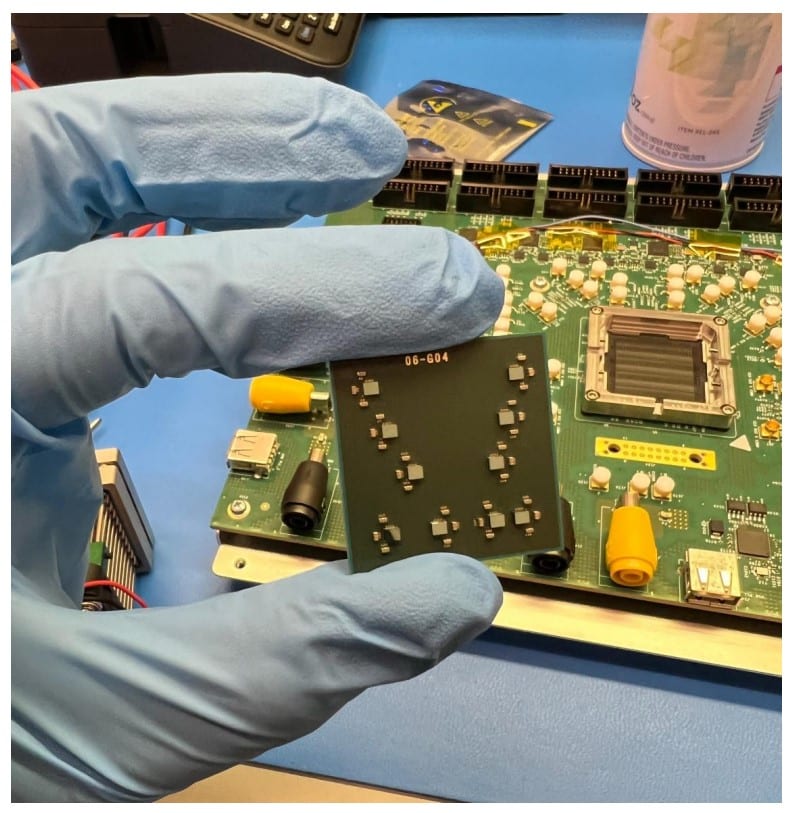
SANTA CLARA, Calif. – May 23, 2023 – Eliyan Corporation, credited for the invention of the semiconductor industry’s highest-performance and most efficient chiplet interconnect, today announced silicon availability for its breakthrough NuLink™ PHY technology. First silicon, achieved in one year from company’s initial funding, validates Eliyan’s UCIe-compatible approach to enabling high performance and highly scalable multi-die architectures for compute-intensive applications.
Implemented in a standard 5nm process from TSMC, the chip operates at 40Gbps/bump delivering over 2.2Tbps/mm of beachfront bandwidth at 130um pitch on standard organic packaging and meets the company’s aggressive power and area targets. The highly area efficient NuLink™ PHY is bump limited and can deliver up to 3Tbps/mm once implemented on available standard packaging technologies at finer bump pitches, leveraging its innovative interference cancellation techniques.
“The economics of adopting a chiplet approach for IC design are tightly linked with the cost and maturity of the interconnect and packaging solution, as we demonstrated in our analysis”, asserts John Lorenz, Senior Analyst, Computing and Software Solutions at Yole Intelligence. “Eliyan’s chiplet interconnect technology will make multi-die approaches more attractive to chip suppliers whose designs must optimize on power and bandwidth vectors. This is especially the case for those in accelerated server computing applications, a market mainly served by datacenter GPU hardware, and which we see sustaining a 22% unit growth CAGR through 20281.”

The successful silicon implementation demonstrates that Eliyan’s technology in standard organic packaging achieves similar bandwidth, power efficiency, and latency as die-to-die implementations using advanced packaging technologies, but without the drawbacks of those complex and expensive solutions. The ability to implement chiplet-based systems in standard organic packages enables the creation of larger system-in-package (SiP) solutions thus higher performance per power at considerably lower cost and higher yield. These factors provide major gains in sustainability as well.
“First silicon with the results and time frame we have achieved is a significant milestone and differentiator in the successful commercialization of our technology. It positions us as the front runner in enabling the most efficient chiplet interconnect in the semiconductor industry,” said Eliyan’s founding CEO Ramin Farjadrad. “With a proven silicon implementation, chip developers will now be able to realize the full benefits of the multi-die architectures without constraints imposed by advanced packaging such as size limitations of silicon interposers. It also enables the practical mix and match of chiplets in different processes and foundries.”
Multi-die architectures are an increasingly necessary approach to handling the needs of compute-intensive applications in data centers, cloud computing, and especially generative AI that require large amounts of memory and fast inter-chip communications. Additionally, a more efficient approach to implementing chiplet products is needed in industries such as automotive and gaming devices, which require much more reliable and cost-effective solutions than what advanced packaging options can offer.
Eliyan’s NuLink technology uses novel implementation techniques to provide significant power-performance differentiation for chiplet connectivity over any packaging substrate, reducing complexity and lowering overall development time and costs. It eliminates the need for silicon interposers, which in addition to being constrained by supply chain issues, limit overall system-in-package size. As a result, the total amount of memory and compute cores in a package ultimately constrain performance, resulting in low yield, increased total cost of ownership, and extended overall manufacturing cycle time.
Eliyan’s chiplet interconnect technology has been the foundation of the Bunch of Wires (BoW) standard (which has already been adopted by the Open Compute Project), and is fundamentally compatible with the UCIe standardization efforts. Eliyan is currently working with standards bodies to create an efficient universal die-to-die interconnect optimized for memory traffic to help accelerate the adoption of memory chiplets.
Silicon characterization data is now available. Eliyan is also in the process of porting its design to multiple foundry and node technologies based on early customer interest and demand.
About Eliyan
Eliyan Corporation is leading the chiplet revolution, focusing on a fundamental challenge with scaling semiconductor performance, size, power, and cost to meet the needs of high-performance computing applications, from desktop to datacenter. It has developed a breakthrough technology to enable the industry’s highest performing chiplet interconnect for homogenous and heterogenous multi-die architectures using standard packaging substrates, enabling increased sustainability through reduction in costs, manufacturing waste and power consumption. The company’s Bunch of Wires (BoW) chiplet interconnect technology, invented by founder Ramin Farjadrad and proven to increase performance by 2x and reduce power in half, provides a more efficient approach to developing chiplet-based architectures – which are the pathway to the continued scaling of Moore’s Law. More information can be found here. www.eliyan.com
For more information, contact:
Mike Sottak
mike@wiredislandpr.com
650-248-9597
1 Source: Processor Market Monitor, Q1 2023, Yole Intelligence