The Ultimate Chiplet Interconnect.
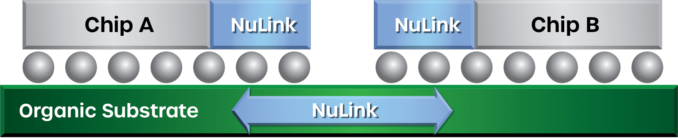
Eliyan’s NuLink™ PHY technology can be optimized for high-speed serial die-to-die connections using any industry standard or custom interconnect scheme. It can deliver outstanding performance at low power in advanced packaging or standard packaging using a wide range of bump pitches.
NuLink’s Evolution
A Breakthrough Die-to-Die Interconnect
NuLink evolved from a 2016 architectural breakthrough in PHY technology. Recognized PHY guru (and Eliyan founder) Ramin Farjadrad recognized that the very different electrical environment between dies in multi-die packages should be reflected in the architecture of the PHY IP that drove the connections. The result was a huge step forward in performance, power efficiency, and area. This breakthrough received strong support from the Open Compute Project (OCP) and was adopted as an industry standard for chiplet interconnect Bunch of Wires (BoW).
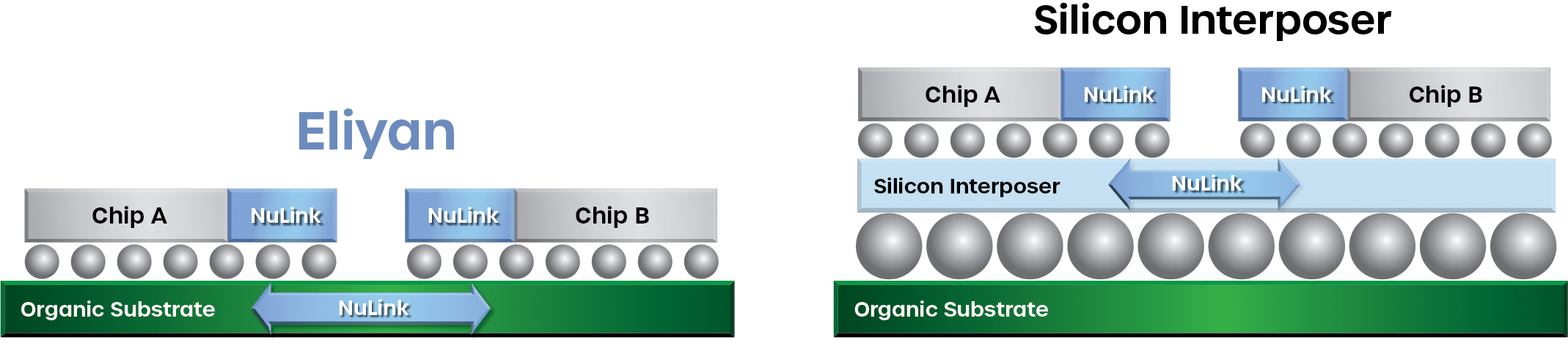
At Eliyan, Farjadrad and his team went beyond the BoW work to further improve and add functionality to the PHY. The result is NuLink. As a protocol-agnostic building block, the NuLink PHY fully supports BoW, the more recent industry standard Universal Chiplet Interface Express (UCIe) and a wide range of other die-to-die interconnect structures. And it supports them on both silicon and organic substrates, at higher performance and lower power than all existing BoW and UCIe standard PHYs.

NuLink for Die-to-Die Connections

NuLink for Die-to-Memory Connections

Universal Memory Interface (UMI™) Connections
Automotive semiconductors are increasingly adopting chiplets to enable multiple configurations for end products. Eliyan’s NuLink solutions can enable high reliability chiplet connections for automotive applications.

Simultaneous Bidirectional (SBD) Connections
Industry Standards

NuLink™ Advantages for Die-to-Die Connections
Simply put, NuLink’s advantages over alternative PHY IP are performance, power efficiency, area, and flexibility. In standard packaging, NuLink can provide the same bandwidth and power efficiency others can only achieve in advanced packaging. And when used in advanced packaging, NuLink offers unparalleled performance.
But this is not the whole story. Unique among all of the die-to-die solutions today, only NuLink technology is capable of simultaneous bidirectional signaling (SBD). Eliyan’s patented technologies and technical know-how enable die-to-die designs that can receive data while simultaneously transmitting data on the same wire at the same time. SBD signaling instantly doubles the bandwidth per interface, enabling the highest possible performance and minimal area for inter-die connections. This is especially important for applications such as AI training and inference for Large Language Models (LLMs).
Target Applications for Die-to-Die
Connections using NuLink
There are specific application scenarios in which NuLink cannot just improve interconnect performance but can change the game for system architects. These include:
- Getting the absolute maximum performance from chiplet-based systems on silicon substrates such as interposers or embedded bridges.
- Implementing a system on a standard organic package substrate—saving cost and ensuring continuity of supply—while achieving similar bandwidth, power, and latency to a silicon-substrate implementation.
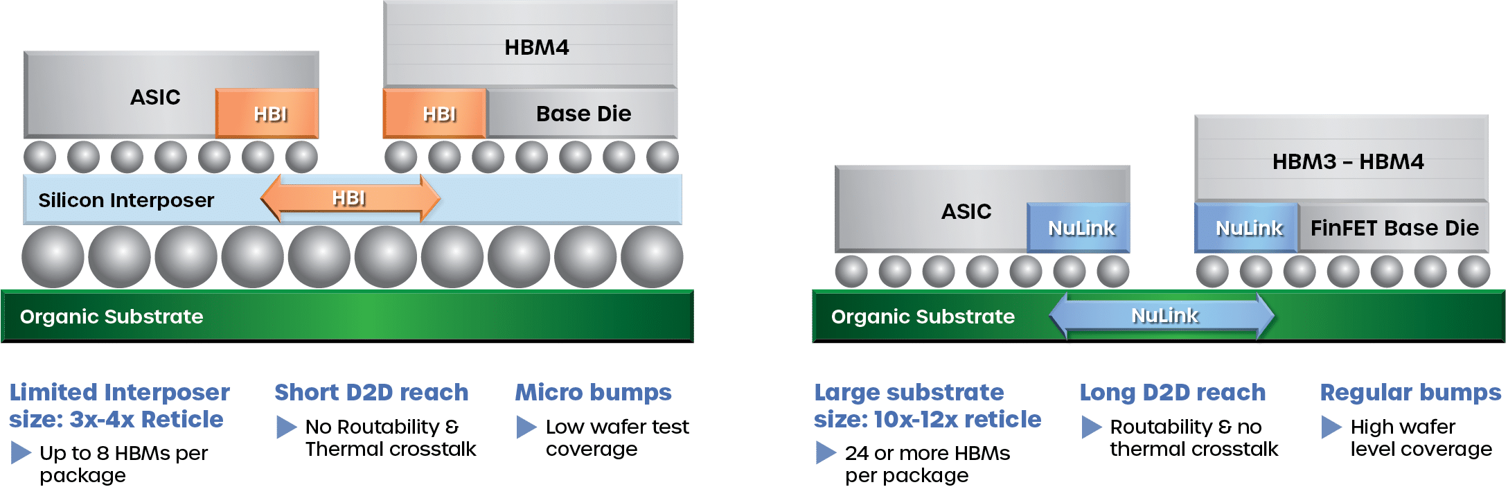
- Exploiting the far larger maximum size of standard organic substrates to integrate a higher number of supporting dies, such as high-bandwidth memory (HBM) and Silicon Photonics chiplets, with ASIC main dies on one substrate.
Getting Multi-Die Designs out of Trouble
The unique capabilities of the NuLink PHY can save system designers from a number of issues that come with advanced packaging:
- Limited maximum area for silicon substrates, limiting the level of integration
- High cost and complexity, forcing high end-system pricing
- Delicate mechanical structures, limiting access to markets such as automotive with mission-critical requirements.
- Long manufacturing cycle time of 3-6 months, creating forecasting and supply issues
- Limited, vendor-specific supply chains, risking continuity of supply
NuLink™ Advantages for Die-to-Memory Connections
NuLink shines in die-to-memory (D2M) applications. NuLink technology natively utilizes bidirectional transceivers for every data lane. In complying with unidirectional standards such as UCIe or BoW, we configure the lanes as unidirectional transmit or receive lanes.
In contrast, memory connections utilize half-duplex bidirectional data lanes which dynamically switch between Read or Write operation, either transmitting or receiving data at any given time.
NuLink’s bidirectional transceivers support this dynamic bidirectional capability with fast switching time. This doubles beachfront bandwidth for memory traffic. As a result, NuLink can deliver the bandwidth requirements for HBM on standard organic packaging with 100um and above bump pitch. We use this NuLink capability in die-to-memory interface proposals such as SPHBM (HBM-ASIC connectivity over standard package) and UMI (Universal Memory Interface).
- High cost, complexity, mechanical sensitivity
- Long manufacturing cycle time
- Limited CoWoS supply chain
- Low cost, complexity, mechanical sensitivity
- Short manufacturing cycle time
- Widely available organic pckg supply chain
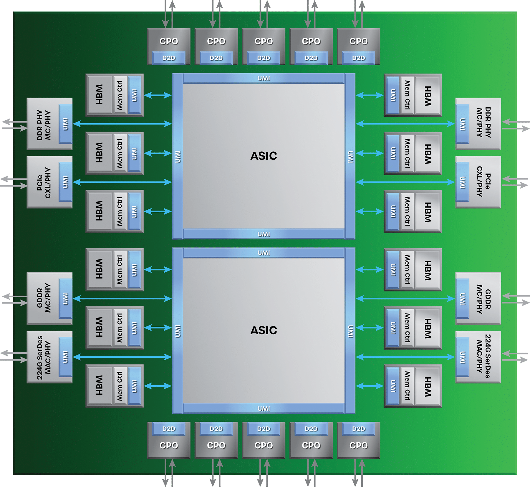
NuLink™ in the Universal Memory
Interface (UMI™)
Eliyan has proposed to industry standards bodies that NuLink-based die-to-die links could be used to define a Universal Memory Interface (UMI). An ASIC with a UMI connection could hit different performance points utilizing different memory chiplets. The figure below shows the concept with a single ASIC design connected to DDR, GDDR, and HBM DRAMs.

Benefits include
- Maximizing the ASIC beachfront bandwidth
- Improving end-system SKU management by enabling different systems with the same ASIC
- Saving power & ASIC area by replacing DRAM PHYs and controllers with more efficient NuLink PHYs and UMI controllers
- Enabling vendors to offer memory PHYs as silicon-proven chiplets (instead of IPs in every new node)
In addition, the UMI concept can make connections to non-memory dies such as co-packaged optics (CPO) and SerDes chiplets.
NuLink™ for Simultaneous Bidirectional
(SBD) Connections
Unique among all of the die-to-die solutions today, only NuLink technology is capable of simultaneous bidirectional signaling (SBD) which means sending data on wires in both directions at the same time. Eliyan’s patented technologies and technical knowhow enable D2D designs that can receive data while simultaneously transmitting data on the same wire at the same time. Using SBD signaling instantly doubles the bandwidth per interface, enabling the highest possible performance for D2D connections, especially important for applications such as AI training and inference for Large Language Models (LLMs).

Benefits
- Highest D2D/D2M/C2C performance—enabling significant AI training/inference improvement in Large Language Models (LLMs)
- Removing the Memory Wall by increasing number of HBMs by 4x in a package—accommodating much larger LLMs models (GPT4, GPT5)
- Extending the reach of interconnect by 10x — enabling much larger and more powerful systems in package (SiP) solutions
- Reducing the time to market of AI ASICs by eliminating the need for Interposer readiness, integration and test by at least 8-12 weeks
- Substantially reducing packaging, test, assembly costs by at least 2x